For user manual and purchasing please visit: https://www.ddzheng.cc/?page_id=666
Table of Contents
Update 13 Feb. 2025:
The first batch run has finished. This will be also PVT. change to reverse mounted 1206 led on bottom side.
Update 29 Jan 2025:
Out of advice from Gearspace user I will add a header footprint for remote mounted button.
I added ability to wake up WiFi using Bluetooth LE. The operation is done by using a smartphone and attempt to connect to the board. The connection will wake up WiFi and at same time kill BLE process in ESP32, this will cause the connection to fail. This is done on purpose so an app is not needed to wake the WiFi, and you won’t have to un-pair the Bluetooth device each time.
Well, here it is
This project has taken too long but it’s finally complete and ready to use and I’ll make everything open source at a later time.
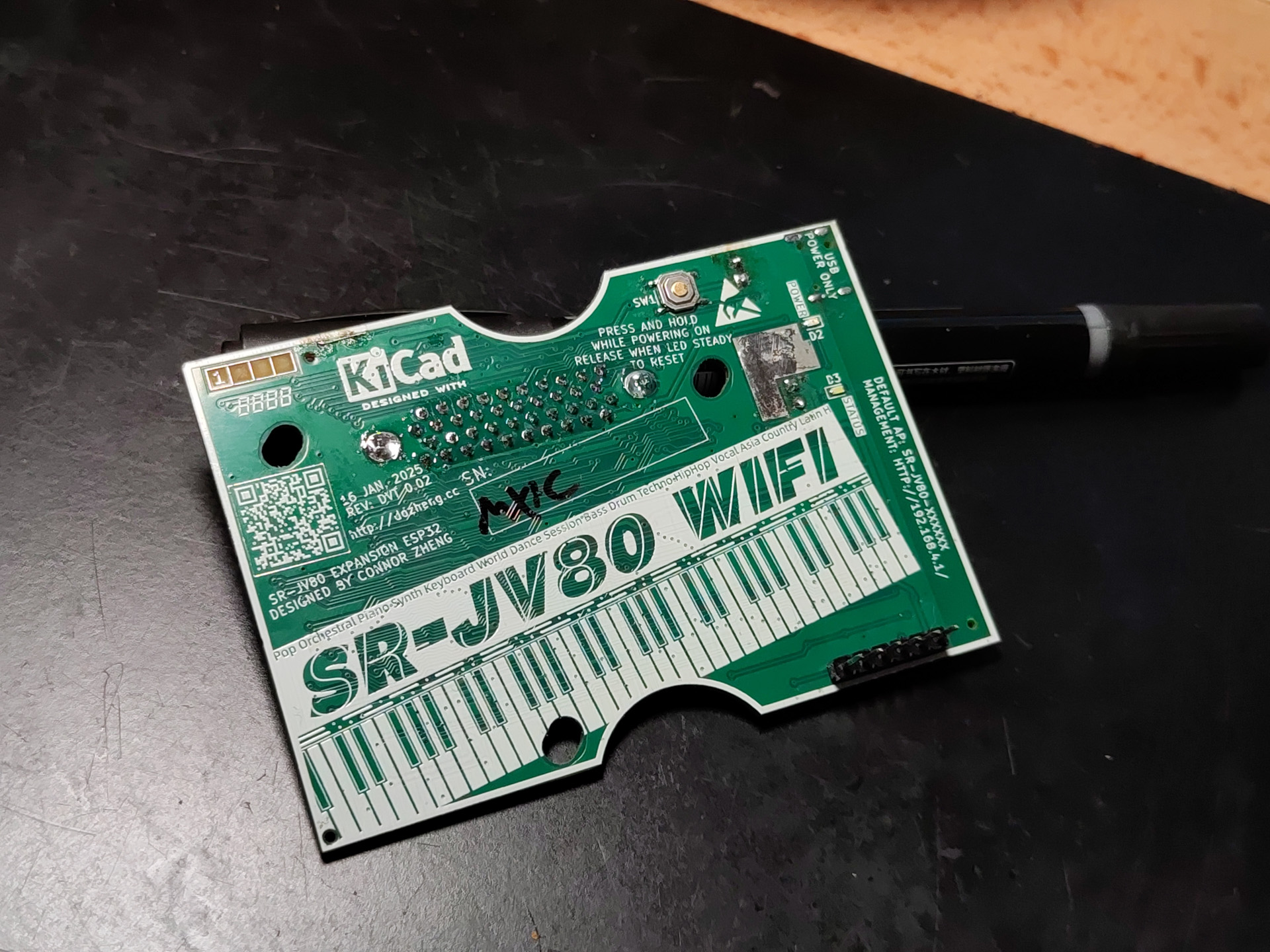
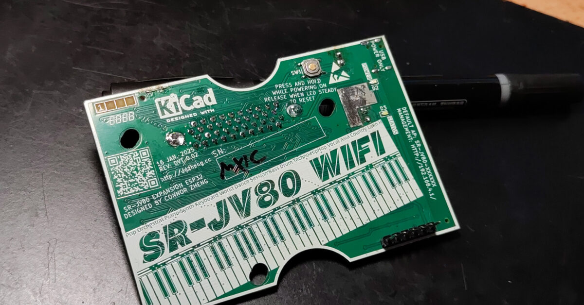
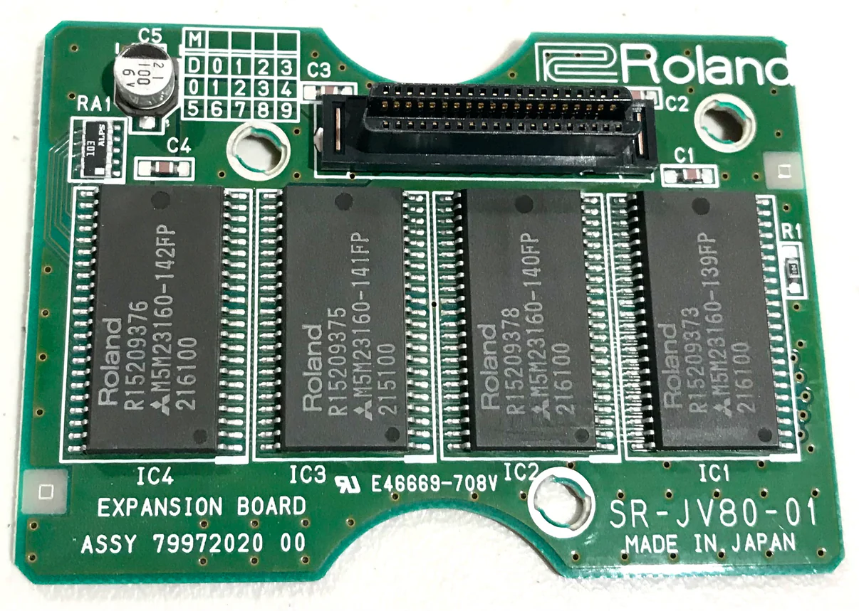
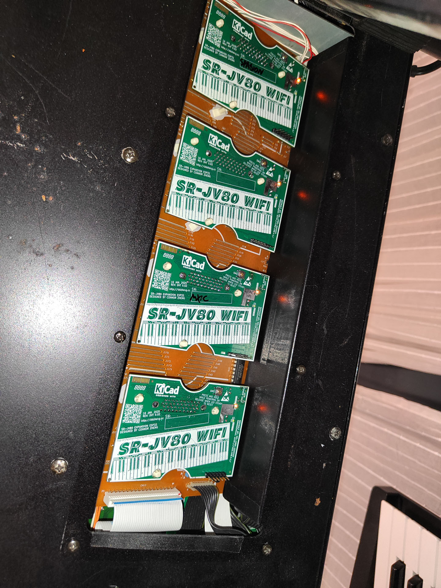
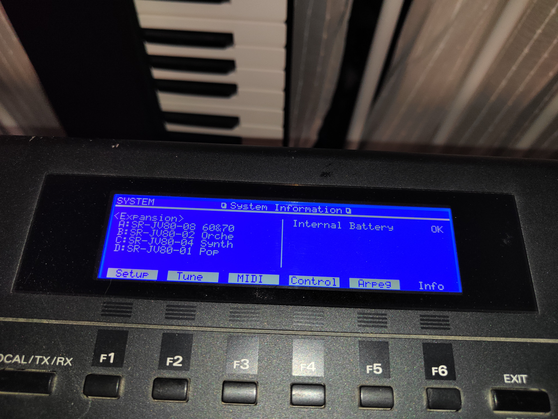
The SR-JV80 Expansion Card
The Roland JV series synthesizer were a legend of their time. Most of those synthesizers can accept 1 or more SR-JV80 series expansion card.
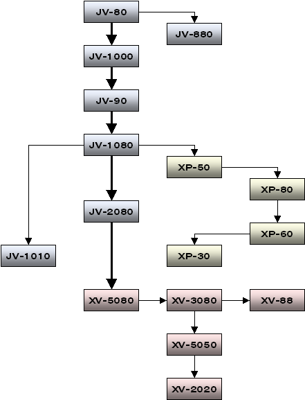
Roland has made some great sounds in these cards. According to most material there are 19 cards made by Roland. As time progresses these cards has become unobtanium and extremely expensive (especially in China, a card usually calls for $60 to $200). A list of expansion card can be seen at Edward DTech’s site: https://www.dtech.lv/techarticles_roland_exp.html
The Roland JV-80, JV-90, JV-1000, JV-880, and JV-1010 synths from the JV series can be expanded with 1 SR-JV80 wave expansion board, as can the JD-990 and the Fantom FA-76. The XP-30 and XV-88 can accept up to 2. The XP-50, XP-60, XP-80, JV-1080, XV-3080, and XV-5080 can accept up to 4. The JV-2080 can accept up to 8.
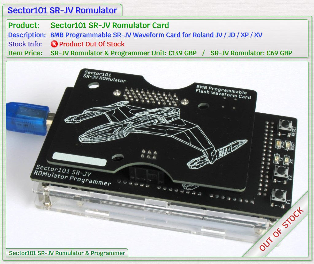
There are products available to act as re-writable SR-JV80 card but they are equally as expensive and from my view, not as user friendly.
Now these cards are relatively simple, they consist of 8MB of ROM and that’s it. It’s connected to the sound generation part of synthesizer via the 40-pin connector. It then act as wave ROM and the sound engine can retrieve samples and patch data from it.
The Project
Blackbox
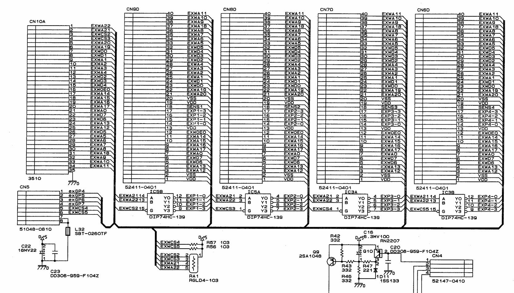
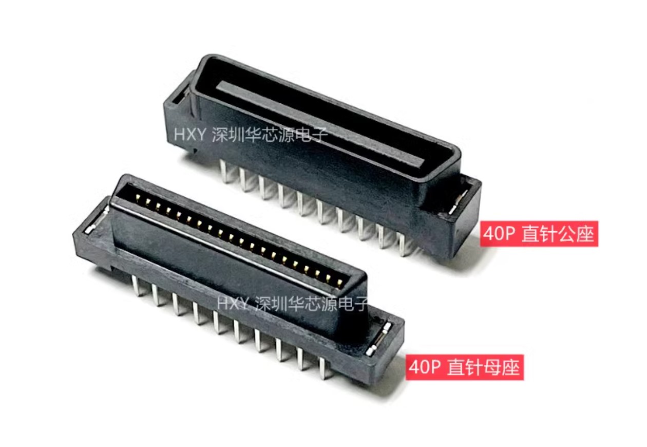
The expansion interface and the synthesizer is essentially a giant blackbox system which we cannot know exactly how it operates. And one thing for sure is that the connector is nowhere to get. After some research I find the SCSI 40-pin all plastic connector which fits the expansion connector perfectly after some filing of the edges.
The connector pinout can be gathered from the schematic and PCB image in service manual.
The physical form factor is another problem. Since I don’t even have a real card on hand, I used some of the high-res photo I found on the internet and used photoshop to correct the image and took some measurement. I then put the drawings in KiCAD.
Defining the System and Design the Schematic
I’ve defined the requirements for this project as follows:
- This product will have a re-writable memory (EEPROM or flash memory, as opposed to mask rom or OTP ROM)
- This product will have a Wi-Fi interface so that one don’t need to remove it from the synthesizer to reprogram it
- It need to conform to the original SR-JV80 expansion card form factor and be able to install in the synth without modifying the synth
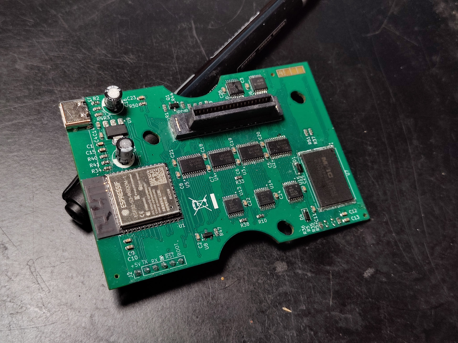
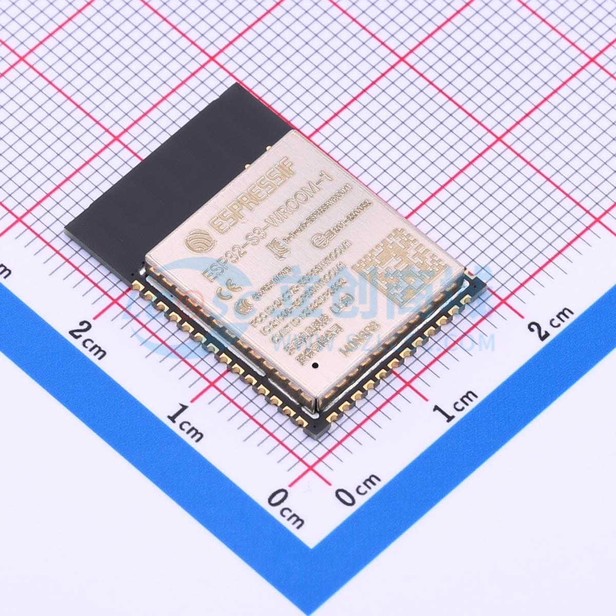
For the main processor, as I’ve previously used Espressif products, I decided to use ESP32-S3 as the processor of the card. I decided on the WROOM module.
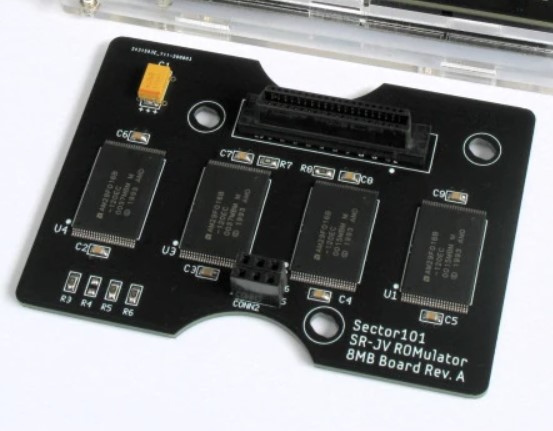
Because the original SR-JV80 expansion card has 4 2MB ROM, the Sector101’s Romulator use the same structure, utilizing 4 flash chips.
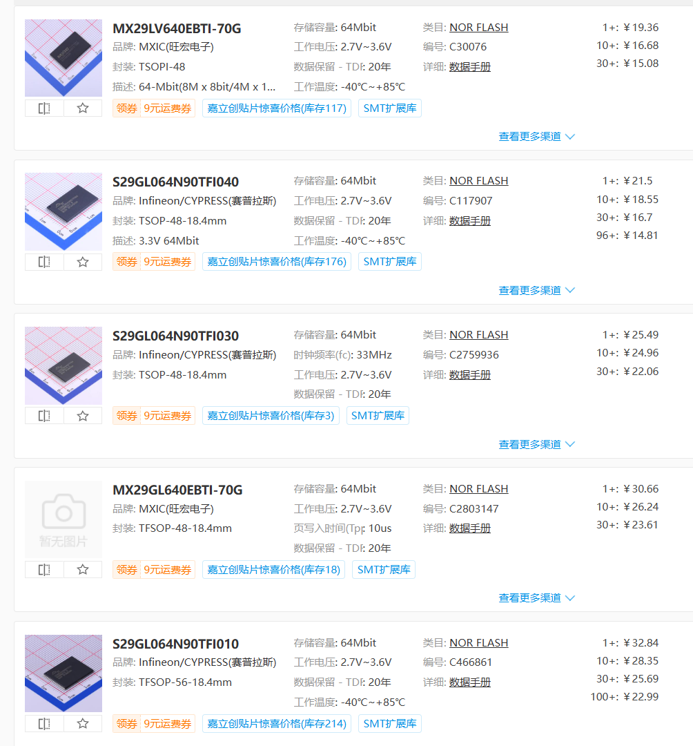
I decided to ditch this solution and use one 8MB(64M) flash. I selected the Cypress (Spansion) S29GL064 and MXIC MX29LV640E.
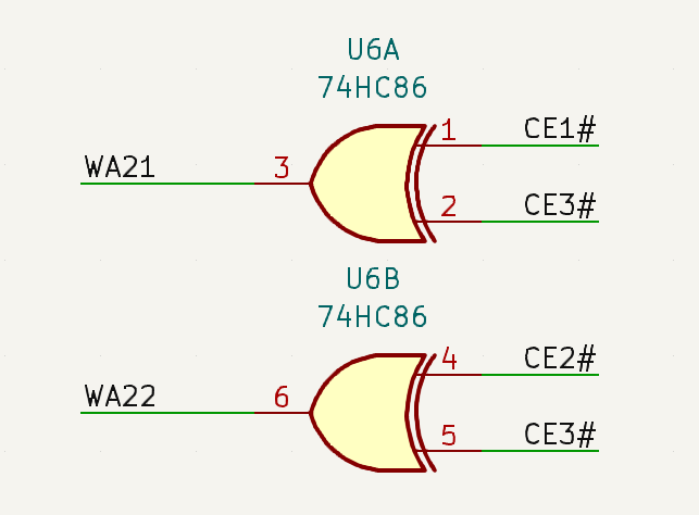
The interface has one chip select line for each chip. This means I’ll need to translate 4 mutually exclusive active low input to 2 active high output (4 to 2 encoder), which can be realized with XOR gate. I selected 74HC86.
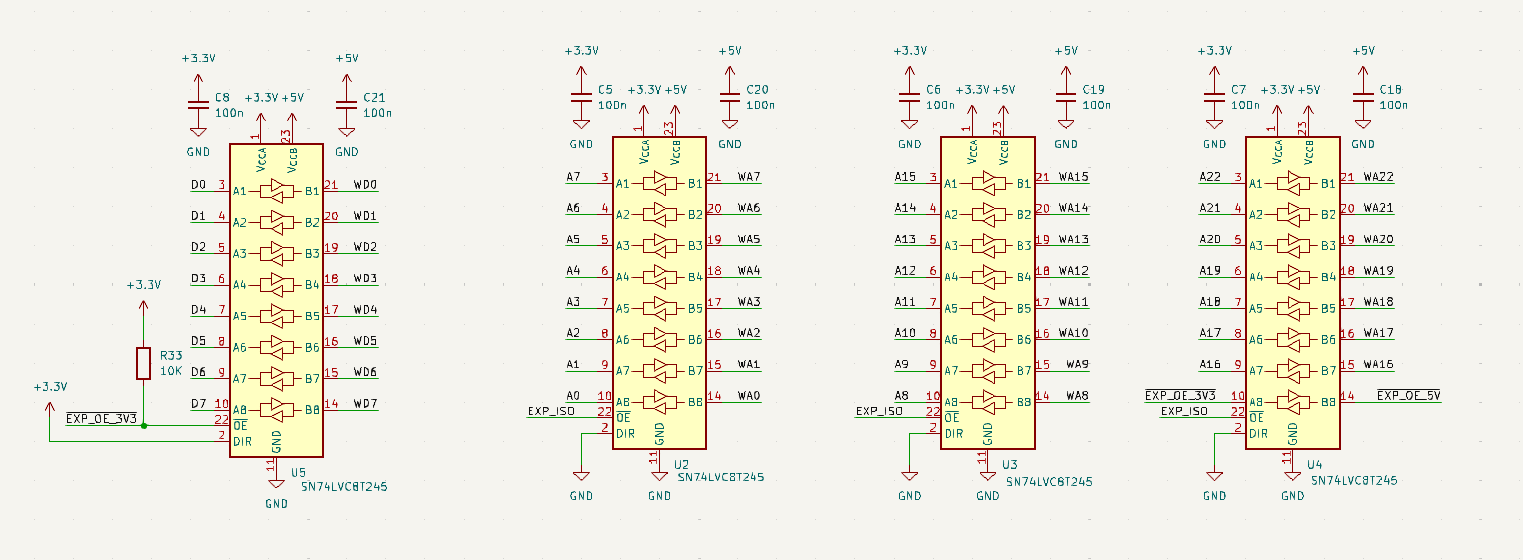
At this capacity level there are only 3.3V flash available, but since I need to be able to isolate the synthesizer interface from the card to be able to program it in-place anyway, this won’t be a problem. The data and address lines on the 3.3V side will connect to processor for erasing and programming. On the 5V side they connect to the interface. This is done using 4x 74LVC8T245.
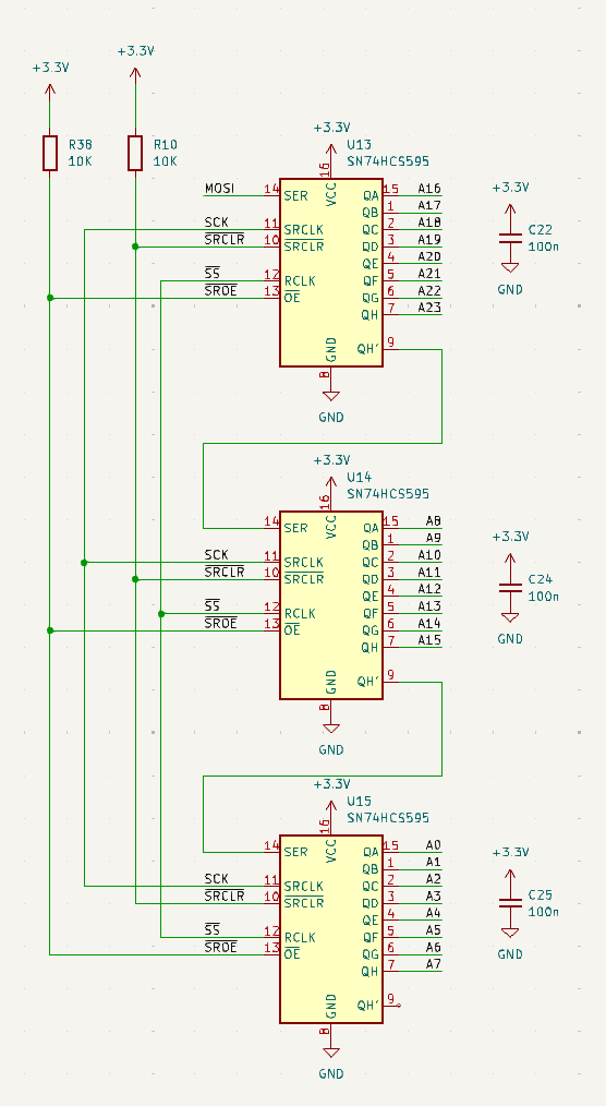
There isn’t enough IO on the ESP32 so I decided on the first version to use a IO expander, which turns out to be way too slow. So I later changed to 74HC595 and eventually 74HCS595. Driving these with the SPI interface it can reach a clock speed of 20MHz or more (Max available from ESP32 is 80M but I don’t think it’s possible with the HCS logic family).
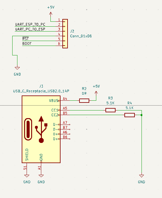
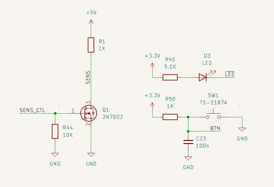
Finally power management with a 1117, a USB port, a program port, a button, 2 LEDs, and a MOSFET for controlling the card present sense pin is added.
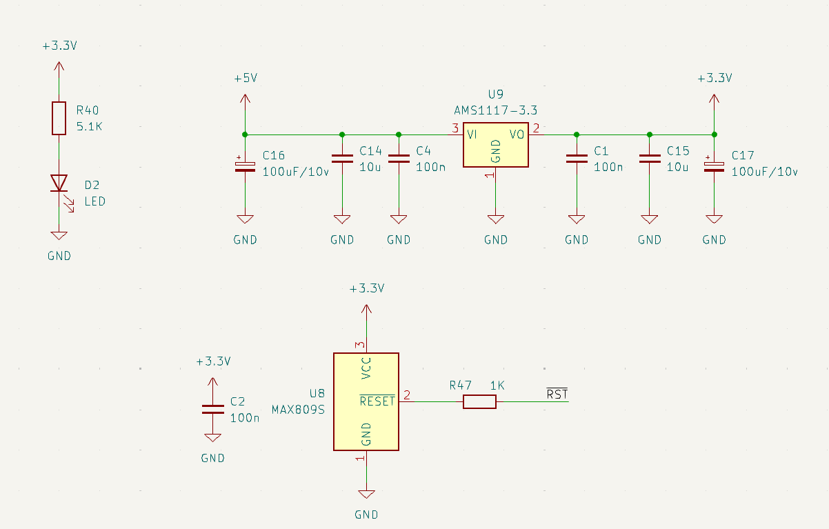
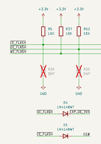
The OE and CE of the flash is configurable to pull-up or pull-down, together with mounting the diodes or not it can control the behavior of the bus controls.
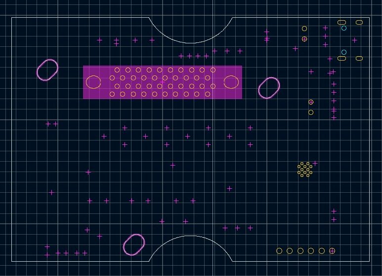
Layout
There are 3 versions as of now:
- Test board version 1 with IO expander. Occupies 2 card slots.
- Test board with 74HC595 and no 74HC08. Occupies 2 card slots.
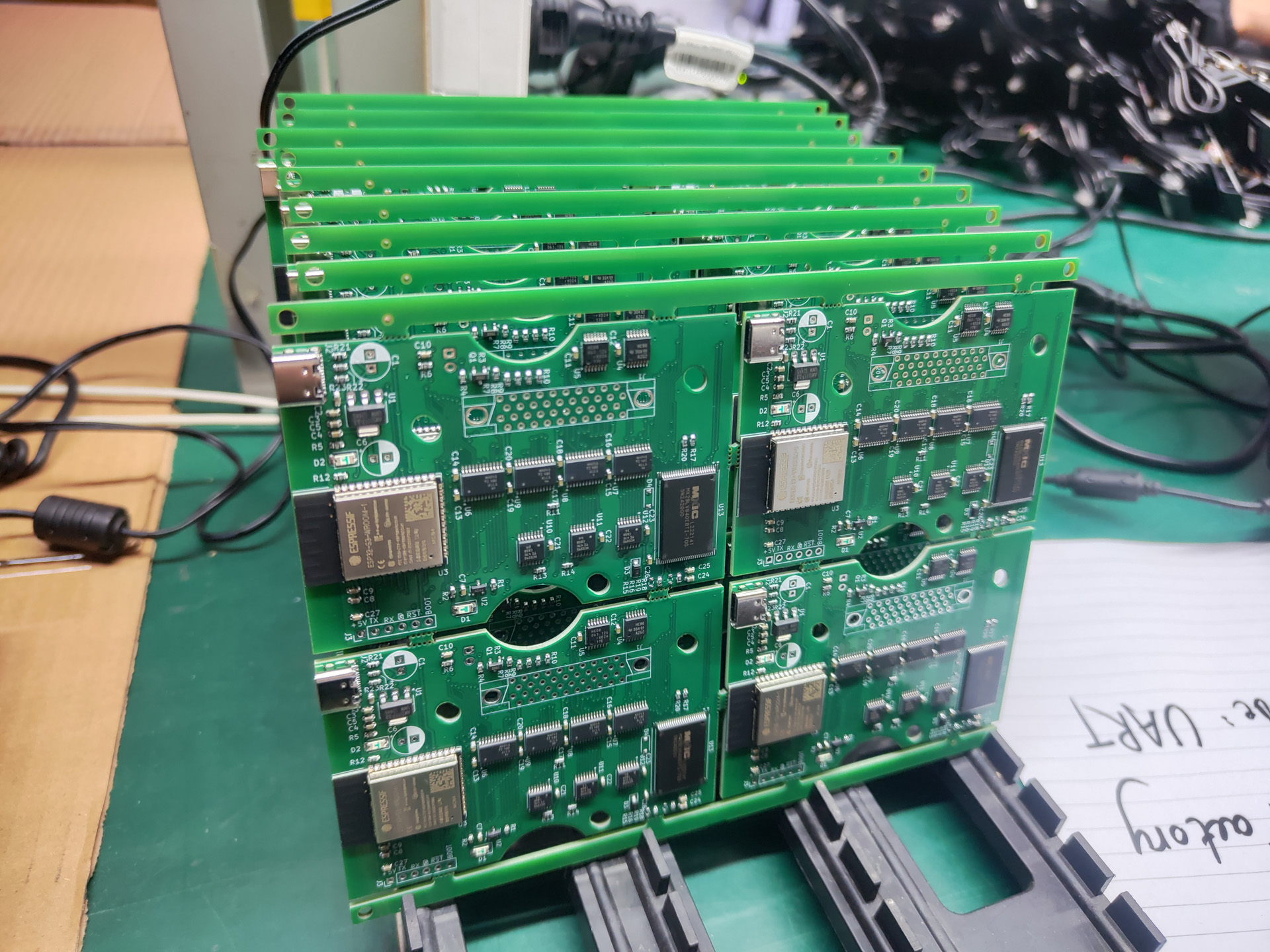
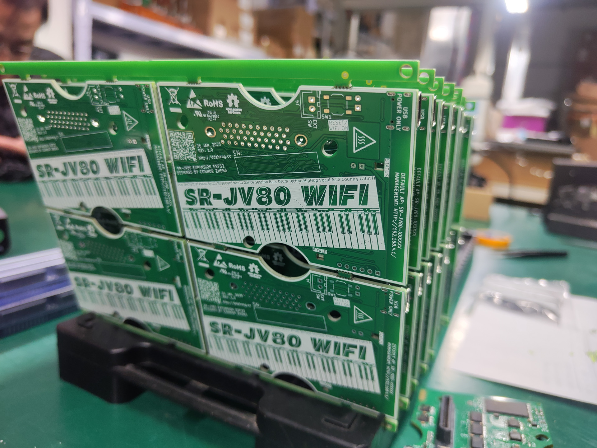
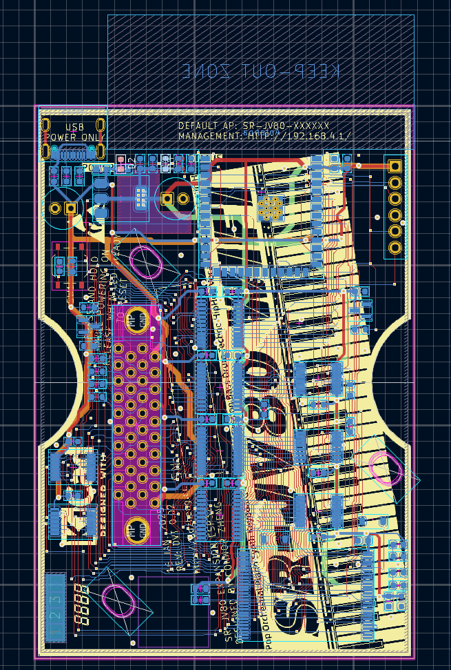
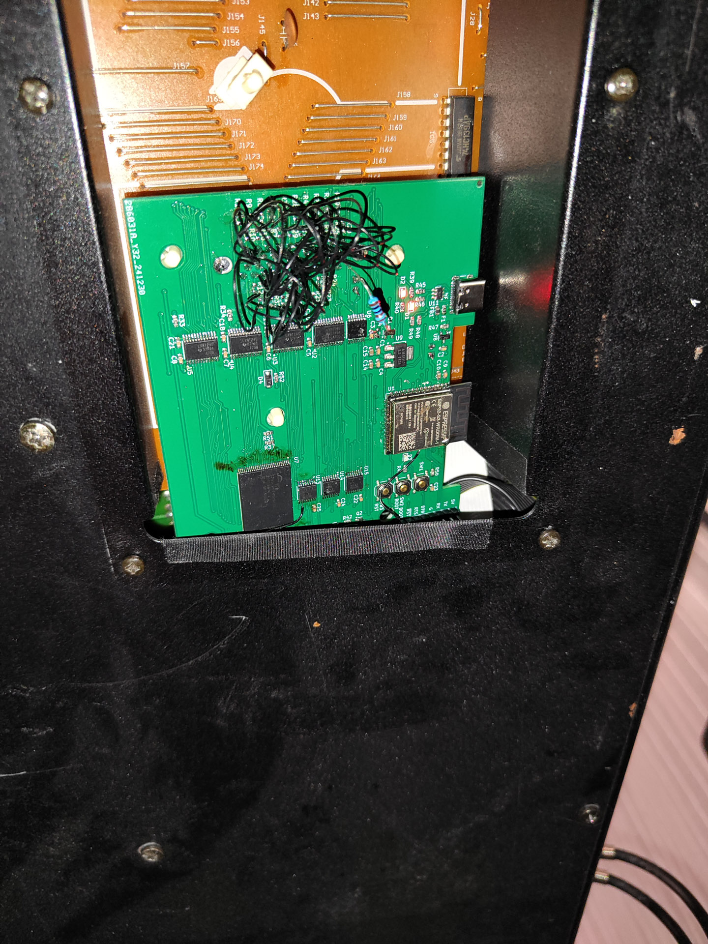
- Board with current design, occupying 1 slot and same profile as real card.
Laying out the board is a painful process as there are so many wires. Luckily with KiCAD’s shove routing and long-lat top-bottom strategy it can be done without too much of a hassle.
For the current version I’m using 4-layer board but it can also be fabricated with 2 layers only since the internal layers are only just power and ground, which is also present on top and bottom layer.
Fabrication and Testing
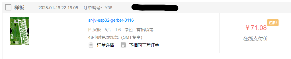
I manufactured the boards at JLCPCB. I have JLCPCB assemble the basic parts like LDO, RCL, and anything else that doesn’t require feeder changing fee in their SMT process.
For testing I bought N8R8 version (8MB Flash, 8MB PSRAM) of the ESP32S3-WROOM.
On the first version (IO expander) I quickly realized it won’t work due to the slow speed of the IO expander. So I quickly spun the next test board version. However under the influence of the scramble scheme of these ROM, I connected the address and data wires all wrong. So I had to airwire all those lines at the 5V side. Luckily I put 0R resistor in series with the 5V signals on the test boards.
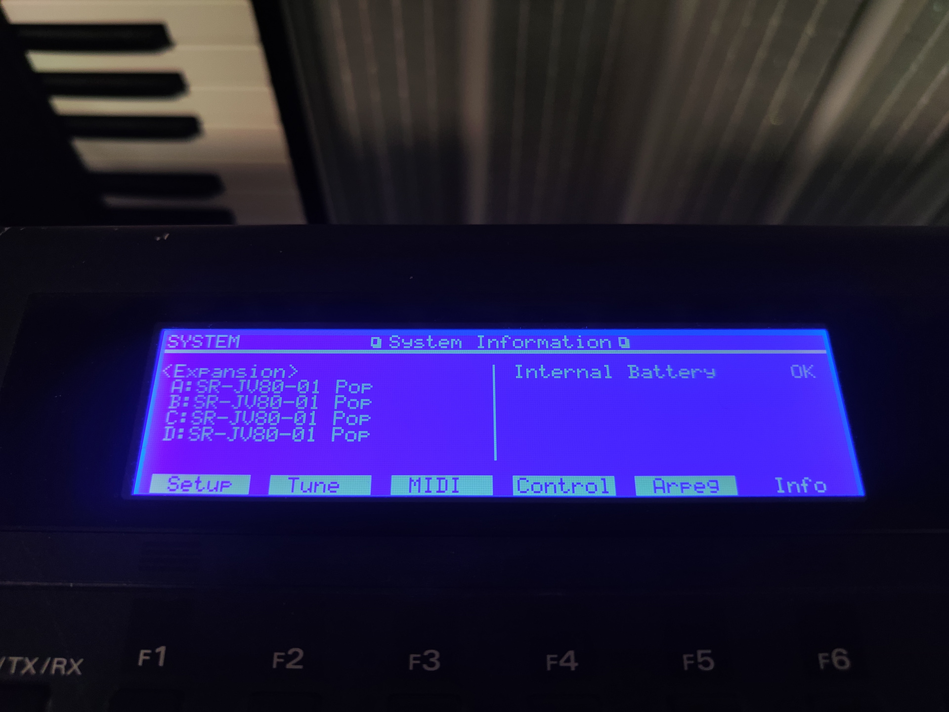
On this version I tested for all functionality and did some signal measurement. On these first versions I didn’t manage the CE lines from the interface however since those are CE lines there are no overall CE available after encoding (can’t distinguish between address 00 or no CE active). This resulted in one card shown as 4 identical cards in my XP-80 due to the WOE line is shared between cards. I only made one test board but there definitely will be bus conflict if more than one card are installed.
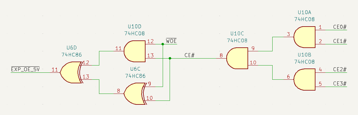
So later on the third version I added a 74HC08 to get a combined CE line, which through a diode control the flash’s CE pin. This is OR’ed with the WOE line to get the card’s OE control, which is fed through the remaining 74LVC245 channel to get a 3.3V OE to control the flash and the data port 74LVC245. The OR’ing is done using the remaining gates of the 74HC86 and 74HC08 to save cost.
Currently this all working just fine. For the production version I’ll probably just tie CE with a pull-down.
Software
This is where I suck. I have previously used ESP-IDF and know something about FreeRTOS but when it comes to real projects it still give me headaches.

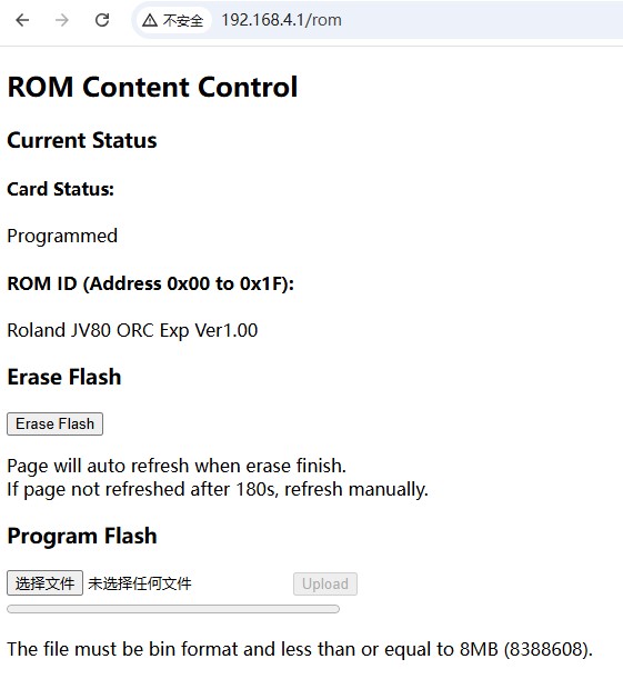
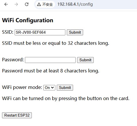
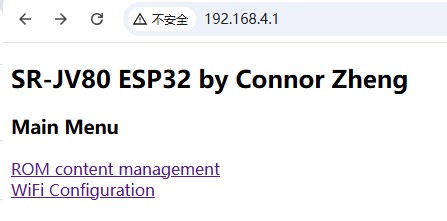
When user connect to the WiFi hotspot and access the ESP32 server, some webpages are served, and the user can erase the flash, upload a new ROM, and configure the WiFi. The WiFi off option is the latest add due to the fear of too high current consumption if someone install all expansion with such card.
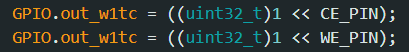
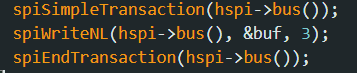
To save cost, some flash I chose does only support byte/word programming. The flash programming is done with IO operations so their speed is very important. I used direct register writes for bus control pins, used dedicated IO to control the data pins (single CPU cycle set 8 pins), and SPI running at 20M clock to control the shift registers for address lines. The current program time for 8MB is 6 minutes.

The programming runs in a task and receive data to program through a queue.
The software reads nvs storage on startup to get WiFi configuration information. It configures data pins, shift register output pins and all bus control pins as tri-state. If the button is pressed on boot and still pressed after 3 seconds, the nvs config will be cleared. If WiFi off is set, a button press will start WiFi and server. When user selects erase or program, ESP32 will set the OE of U2, U3, U4 high through IO1 so their outputs tri-state. The OE of U5 will also tri-state due to pull-up. This way the expansion port is isolated allowing programming of the flash in-system.
I chose to only include off and on option, rather than more options like off after x minutes, because if the 5V supply is not enough, the WiFi of multiple installed card cannot start simultaneously anyway, so it has to be off on boot and be later woken up manually.
Overall Result
Currently everything is working. I’ll do some more testing and probably will spin a small batch for PVT sale. After I’m confident enough with the design I’ll release those as open source.
Would like to purchase one please 🙂
It’s now out of stock as of Mar 22. Please subscribe to the stock availability notification, thank you
That sounds very, very good, i always dreamed to make a card by my own..!!
Hello,
I’m totally interested in a few of these cards, I have one JV1080 and one JV2028.
Been using one of the Sector101 cards to load patches on my units but the whole
process of opening the units is not something I enjoy doing to say the least.
Let me know availability and price.
Thanks in advance
Hi LdF, you can now purchase card at https://www.ddzheng.cc/?page_id=666
If you need more than one or two cards, please order 1 or 2 first and order more when next batch is available. I’ll give you discount then.
Greetings
this is awesome. Would be really interested in purchasing a few of these!